KINIRO ULTRA Installation Guide
Disclaimer: This is a first draft and will be amended. There are placeholder/missing photos that will be replaced or added later.
Kiniro Kit Contents
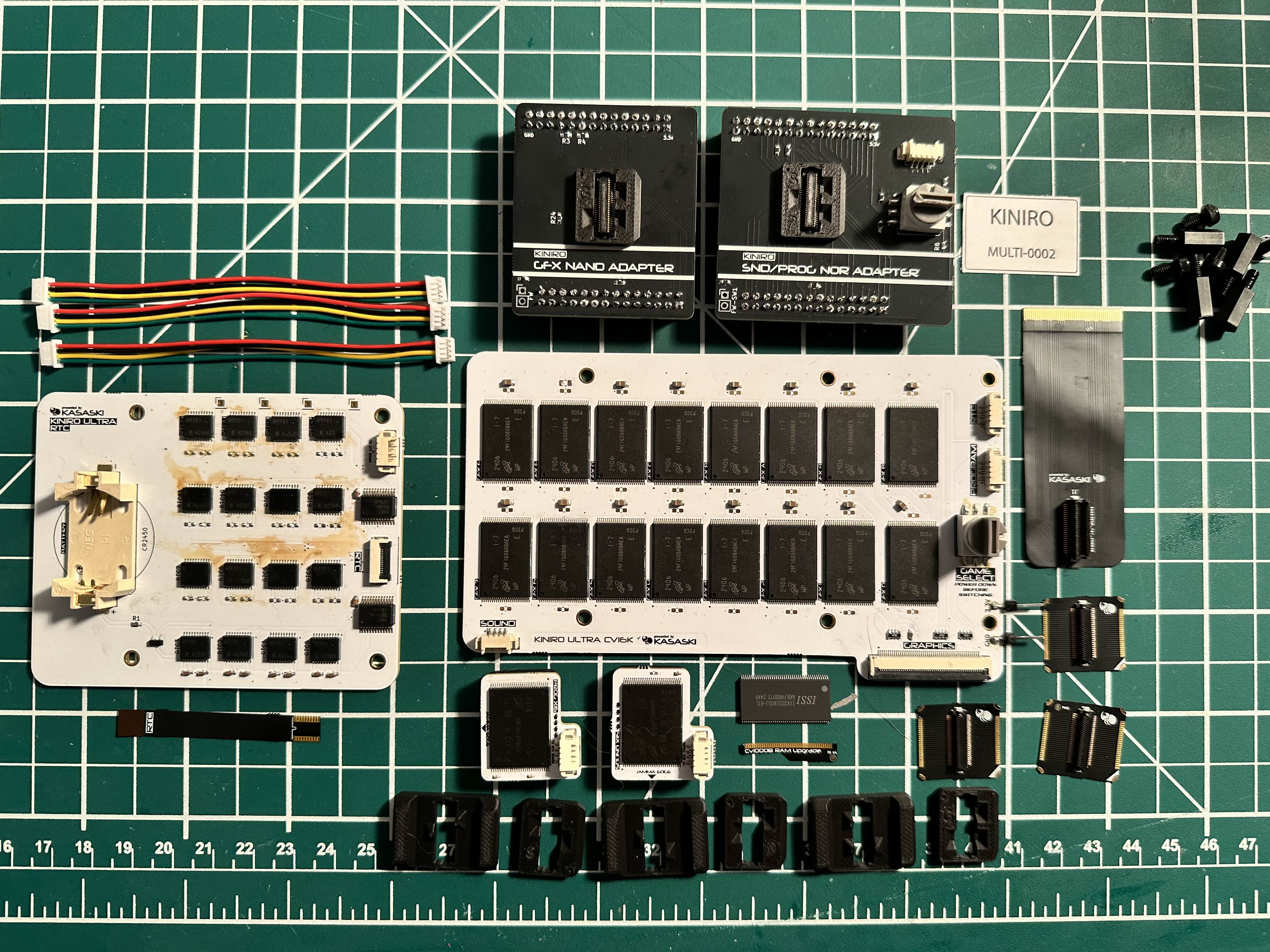 *prototype is pictured. Photo to be updated with final (and clean) boards later.
- 1 x Program x16 board
- 1 x Graphics x16 board
- 1 x Sound x16 board
- NOR and NAND Programming adapters
- 2 x 4pin PicoBlade cables
- PCB Stand-offs
- 1x KINIRO serial sticker
- 3x parasite PCBs (labelled SOUND, GFX and PROG)
- 3D printed keyed connectors to ensure correct installation orientation
Optional RTC Addon:
- RTC x16 PCB
- RTC ribbon cable
- an additional 4pin PicoBlade cable
If required, a RAM upgrade is provided.
- IS42S32400J-6TL
For the installation, I highly recommend a hot air setup for the removal of the chips. Using something like chipquick de-soldering alloy does work, but it can be messy and makes the process much longer. Clean up flux between each soldering job as you go to keep your PCB tidy.
Installation
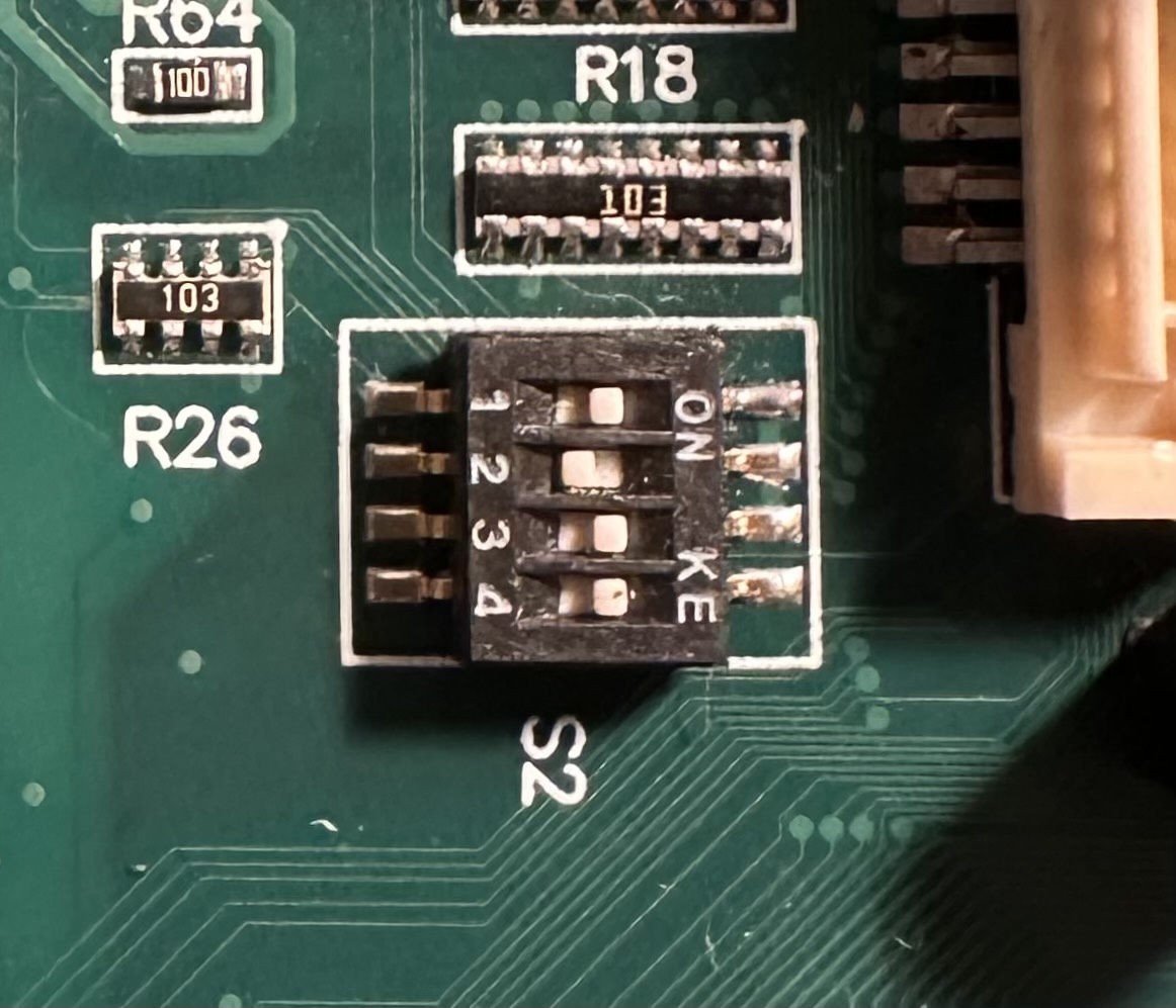
Before you begin I recommend setting dip 2 to the left. With this change you can now toggle special modes with a button combo on a select few games during their boot sequence. This dip will be difficult to access after the install.
Ram Upgrade
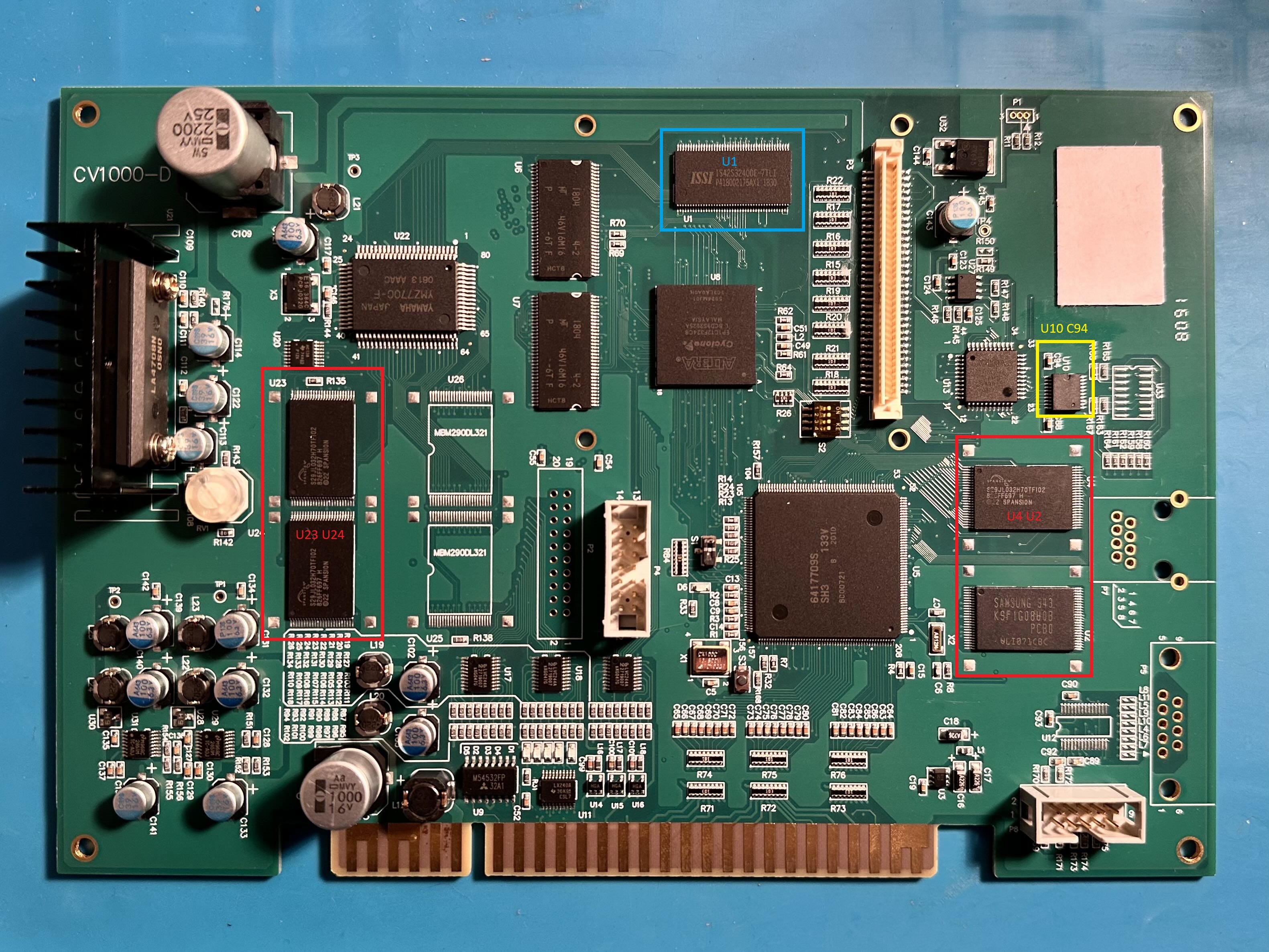
1) Remove U1 and install the IS42S32400J-6TL in its place (circled in blue)
Program, Sound and GFX Parasites
1) First thing to do is to de-solder the rom chips. You will remove 4 chips in total (circled in red):
- U2 (GFX)
- U4 (PROGRAM)
- U23, U24 (SOUND)
2) Once removed, remove any excess solder on each footprint with solder wick, and clean the area thoroughly of any flux.
Each parasite board is made for a specific rom module but the installation process is identical. Please ensure you get this correct. Each PCB is labelled.
- GFX -> U2
- PROG -> U4
- SOUND -> U23
Please refer to the photos for their correct orientation.
The following steps require precision. Please take care to understand the whole process before beginning.
Repeat steps 3-8 for each of the three parasite pcbs.
3) Apply some fresh solder to the rom footprint, this will help with soldering later.
4) On the underside of the parasite pcb you will see double sided tape, remove the protective film. With the tape exposed, double check the PCB is correctly orientated (check the photos above).
5) !!BE CAREFUL!! Once the tape begins making contact with the donor, removal can damage the parasite pcb. Carefully align the pads of the parasite board with the pads of the rom footprint on the PCB. It is best to align one side of pads and slowly angle the pcb in place to align the other side. Take extra care to ensure all pins are aligned correctly.
6) Once it looks good, gently but firmly press down on the header connector to bond the double sided tape and set it in place. You should have a tiny amount of play with the tape to get perfect alignment if it moved at all during bonding. You can also use something like a q-tip to help bond the tape by rubbing it over the parasite pcb surface
7) With a small amount of flux, you can now solder the pads of the parasite to the footprint using a soldering iron.
8) On each corner of the parasite board, there should be grounding pads that align with pads on the donor pcb. Please solder these for a more stable install. You may need a fair amount of heat as the ground plane will suck heat away quickly.
9) With each pcb now soldered in place, you can install the 3D printed keyed connectors. These are essential to ensure the pcbs are not installed into the wrong place and prevent the pcbs from being angled and damaging the connector. Please refer to the photos below:
RTC Module
1) De-solder U10 and C94 (this cap is not required any more and gets in the way). Please refer to the reference picture at the beginning of the instructions, they are circled in yellow.
2) Orientate the RTC ribbon cable so that the text “U10” and the little beetle is facing upwards, away from the PCB (refer to picture)
3) BEFORE INSTALLING put the ribbon cable in position and make a 90 degree bend as shown. The cable should now sit just slightly above the top pins of U13.
4) Align the pads and carefully install with a soldering iron.
5) Install the shorter PCB stand-offs into the 4 mounting holes surrounding U8, to the left of U10.
6) You can now install the RTCx16 PCB onto the stand-offs, using the longer stand-offs to secure the PCB. Ensure the 4 pin ‘TO GFX’ header is facing towards the right
7) Connect the U10 ribbon cable to the RTC module.
8) Connect the 4 pin picoblade cable to the ‘TO GFX’ header.
9) Optionally install a battery, but time keeping is pretty much useless.
Programming
For programming, please refer to my programming guide
Final Assembly
We are done with soldering!
If you haven’t installed the RTC module, install the longer stand-offs to the 4 mounting points around U8. Also remember to install your KINIRO serial sticker 🙂.
1) Prepare the Sound x16 and Program x16 pcbs by connecting the 4 pin PicoBlade cables if you haven’t done so already.
2) Prepage the Graphics x16 PCB by connecting the “GRAPHICS” ribbon cable if you haven’t done so already.
3) Install the program x16 pcb onto the PROG parasite PCB, with the “to JAMMA edge” arrow pointing towards the JAMMA edge
4) Install the GRAPHICS PCB on to the stand-offs with the 4 plastic screws. Carefully manoeuvre the graphics ribbon cable to connect it to the GFX parasite PCB.
5) Install the Sound x16 pcb onto the SOUND parasite PCB, with the “to JAMMA edge” arrow pointing towards the JAMMA edge.
6) Connect each of the picoblade cables to their relevant headers.
Congratulations! You’ve completed your install of the KINIRO ULTRA. Each game will be in a state as if theyre brand new, so various unlocks may still require the code being performed.
To register for interest in the kiniro project please fill out the survey!